
Data Acquisition System for High Voltage Recording
Device Description
This device is intended to record high-voltage transient signals during the tests in high-voltage laboratories. Such a device could well be used for testing the “variable resistance dischargers” under high voltages.
Acquisition and Digital Processing
The voltage waveform applied in this type of high-voltage tests is shown in Figure10.1: amplitude below the discharging level is rising to reach the discharging level within some five seconds (point A). Following the discharging point the test voltage is set to zero within at most 0.5 seconds.
The discharging process induces in the test equipment a current pulse in point A; that pulse is used as an external trigger. The sampling data in the pre-discharging point should be compressed and thus will be recorded only the extreme points of the wave. The sampling in the discharging area must be accurate and will be done at the highest rate.
Taking all that into account, was defined two separate recording areas along the waveform, see Figure 10.1:
– The “Extreme Area”, where the amplitude of the test signal is rising up to the discharging point (A), where only the extreme points are stored in order to reconstruct later the wrapping curve of the signal;
– The “Window Area” is placed around the discharging point (A). That area is sampled at the highest rate and all samples are stored in order to have an accurately representation. The window area contains the “pre_discharge zone” and the “post_discharge zone” with respect to the discharging point (A).
To accomplish these demands the device samples the signal at the highest speed while storing the samples in a circular buffer called “Window Memory”. Data stored in the window memory are circularly shifted until the discharging point is reached; at this moment the acquisition stage comes to an end. It will be followed by an off-line processing stage. During the acquisition stage, the device detects the waveform extreme points and stores them into another circular buffer called “Extreme Point Memory”.
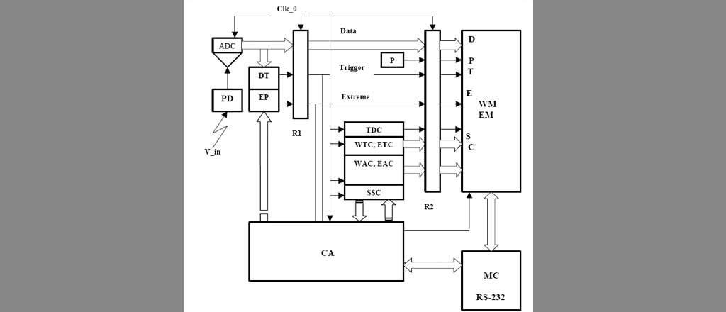
The Architecture
The device contains two acquisition channels (CH0 and CH1) and one microcontroller (MC) connected to a host computer via a serial interface RS232 (see figure_10.2).
Each acquisition channel is made up of an analog to digital converter (ADC), a “window
memory” (WM), an “extreme point memory” (EM), a “control automaton” (CA) for the
acquisition process and a set of control status registers (R).